چکیده:
In this paper, a comparison between CMOS and MOSFET base circuits HSPICE is done with
software. 0.13 CMOS transistor model for simulation and CNTFET Model of Stanford
University used. In simulations amounts of power, circuit delay and PDP is calculated and
these values were compared at the end. And tried to CNTFET applications of transistors in
circuit design, including memory and logic circuits Ternary be expressed.
خلاصه ماشینی:
Evaluation and Comparison of CMOS logic circuits with CNTFET Mahsa Sedaghat¹*, Mahdi Salimi² ¹:Young Researchers and Elite Club, Ardabil Branch, Islamic Azad University, Ardabil, Iran, mahsa.
Figure 3: CMOS inverter circuit and transistor size network display pg and pd.
(a) (b) (c) Figure 4: (a) Chart based on changes in average power consumption w, (b) Chart delay (td) in terms of changes w, (c) PDP graph according to w.
Table 2: minimum amount of delay and average power inverter circuit PDP.
3. NAND Simulation with CMOS In this circuit, the optimal w obtained for the least PDP the inverter circuit, respectively (w = 2.
Figure 7: CMOS Circuit of NAND and display the size of transistors networks pd and pu.
The inverter circuit transistor size network CNTFET pu and pd are the same shape (Fig. 8).
Figure 8: circuit transistor inverter with CNTFET and display size networks pd and pu.
Table 5: Values obtained minimum delay, power and PDP with Swipe L.
10 that respectively delay, average power and PDP are, for Lgate=16n and Swipe obtained tube and minimum values in the table 6 is given.
Table 6: Values obtained minimum delay, power and PDP with Swipe tube.
Figure 13: NAND Circuit with CNTFET and display the size of transistors networks pd and pu.
Table 9: Comparison of the results obtained from simulations GATE CMOS Technology CNTFET Technology Td Avg power pdp Td Avg power pdp INVERTER 7.
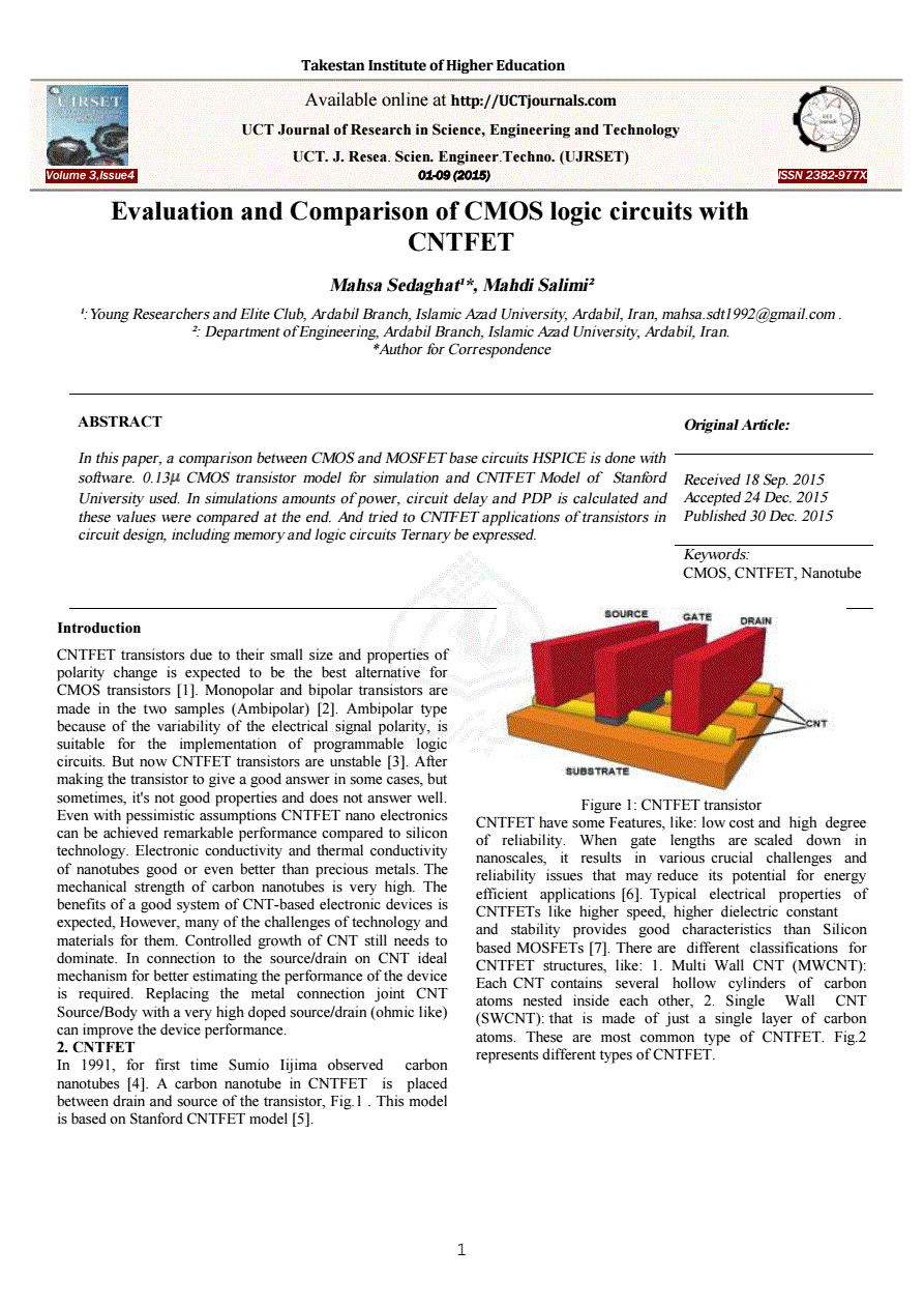
Designed inverter logic gate three (ternary) with transistors CNTFET 6.